
LIQUID CRYSTAL BASED RECONFIGURABLE ANTENNA ARRAYS
Onur Hamza Karabey
1
, Saygin Bildik
1
, Carsten Fritzsch
1
, Sebastian Strunck
1
, Alexander Gaebler
1
,
Rolf Jakoby
1
, and Atsutaka Manabe
2
1
Microwave Engineering Group, Technische Universitaet Darmstadt, Merckstr. 25, 64283, Darmstadt, Germany,
2
Merck KGaA, Liquid Crystal Division, Physical Department , Frankfurter Strasse 250, 64293, Darmstadt, Germany ,
Email : karabey@mwt.tu-darmstadt.de
ABSTRACT
This paper presents reconfigurable antenna arrays based
on liquid crystals (LCs) for earth and space applications.
Tunable reflectarrays at 35 GHz and tunable phased ar-
rays for Ku- and Ka-bands are discussed in detail in
terms of technology, performance, size and cost. Partic-
ular attention is given to LC based cost effective planar
phase shifters in order to design multilayer reconfigurable
phased array antennas applicable for, i.e., automotive ap-
plications.
Key words: Microstrip antennas, liquid crystal devices,
phase shifters, reconfigurable architectures, tunable cir-
cuits and devices.
1. INTRODUCTION
The shortage in the available frequency spectrum for ra-
dio communications and the requirement for more func-
tionality in smaller volume increase demand for recon-
figurable components. Depending on the device re-
quirements there are different possible solutions like PIN
diodes, MEMS or tunable dielectrics to design agile RF
components. Regarding high and continuous tunability,
low/moderate dielectric losses, high linearity and cost
efficiency, liquid crystals (LCs) are promising tunable
materials for microwave applications [1]. Tunable mi-
crowave devices like patch antennas [2], filters [3] and
waveguide structures [4] have been designed and fabri-
cated using LCs. These prototypes also showed that rela-
tively simple and low manifacturing cost make LCs very
attractive for commercial applications.
This paper presents the state of the art for LC based re-
configurable antenna arrays: Realized structures and their
performances. In the following section, properties of LCs
are introduced and dielectric anisotropy of this material
is explained for a typical application. In part 3, recon-
figurable reflectarrays are discussed for their fabrication,
working principle and measurement results. Another type
of antennas that is reconfigurable phased array based on
LCs is presented in part 4. For the phased arrays, pla-
nar phase shifters are key components. Therefore, differ-
ent topologies of planar phase shifters are presented and
compared, in terms of performances and sizes. Particular
attention is given to how LC phase shifters affect critical
antenna parameters, like gain, beam steering speed and
wide range of scanning. Finally, characteristics of a LC
based microstrip patch array are studied.
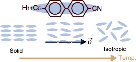
2. PROPERTIES OF LIQUID CRYSTALS
Depending on the temperature liquid crystal phase ex-
ists in a mesophase between a crystalline solid and an
isotropic liquid [5] as shown in Fig. 1. In this state,
the material can flow like a liquid but at the same
time molecules have orientational order. A typical LC
molecule has a rod-like shape as shown in Fig. 1. The
size of the molecule is typically a few nanometers. This
shape anisotropy causes anisotropy in terms of the dielec-
tric constant, as will be described in the following.
Figure 1. Schematic of a typical LC molecule (K15) and
its temperature dependency
A cross section of an LC based inverted microstripline
(IMSL) is shown in Fig. 2. Similar to LCD technology,
there are two substrates for electrodes. The microstripline
and ground electrodes are patterned on top and bottom
substrates respectively. LC is filled between these two
substrates which forms the dielectric of IMSL. For LCs,
the average direction of the long axes of the molecules is
defined as the director, namely n (Fig. 1). Depending on
the RF field distribution and n, LCs feature anisotropic
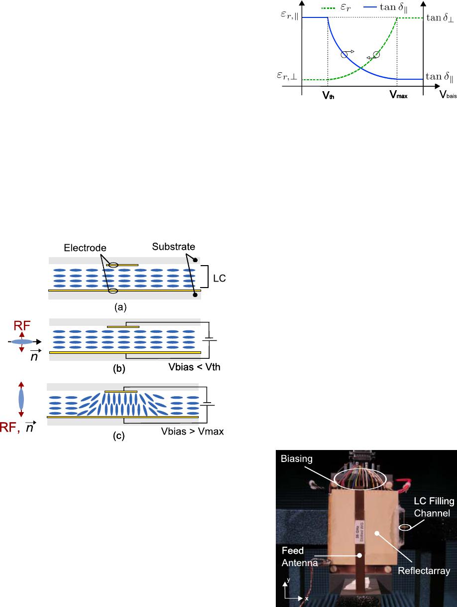
electrical properties. Thus, LC orientation determines
electrical properties of the IMSL. The surfaces of the sub-
strates are coated with a thin polyimide film. This causes
to orient LC molecules parallel to the surfaces initially.
In this case, the RF field distribution is perpendicular to
the director n as shown in Fig. 2b and therefore the rela-
tive permittivity and loss tangent along the short axes are
effective. These are ε
r,⊥
and tan δ
⊥
. Molecules can keep
their orientation if the applied bias voltage is smaller than
the threshold voltage. On the other hand, if the applied
voltage exceeds a certain voltage (Vmax) which depends
on LC, all molecules are aligned parallel to this bias volt-
age (Fig. 2c). Then, ε
r,
and tan δ
become effective.
When the voltage is released again, molecules return to
the initial state due to the polyimide film (Fig. 2b). Re-
quired time for this process is defined as switching time
which depends on LC material, its thickness, temperature
and orientation mechanisms. All other states between
ε
r,⊥
and ε
r,
, equivalently continuous tunability, can be
achieved varying the applied voltage between the thresh-
old voltage and Vmax.
Figure 2. Cross section of an Inverted Microstripline
(IMSL)
All LCs studied up to now have positive anisotropy
for frequencies higher than 0.5 GHz, which means
∆ε
r
= ε
r,
− ε
r,⊥
> 0, and also for LCs the re-
lationship tan δ
⊥
> tan δ
holds true. Such a general
characteristic of LC that is dielectric constant and loss
tangent versus bias voltage is plotted in Fig. 3.
3. RECONFIGURABLE REFLECTARRAYS
Liquid Crystal based reconfigurable reflectarrays are
studied first by Marin et al. [6] and then in [7, 8, 9] for
Ka- and lower W-bands. Required technology of a re-
flecarray fabrication is similar to the IMSL application
explained in the previous section. For this manner, in-
stead of fabricating a microstripline on the top substrate,
Figure 3. High frequency ε
r
and tan δ characteristics of
LC material versus bias voltage
microstrip patches are realized here as antenna elements.
Such a reconfigurable reflectarray is designed based on
the principle of variable patch dimensions [10]. Instead
of changing the dimensions of the metalized patch, di-
electric properties of LC under the patches are tuned with
a bias voltage less than 20 V . Hence, although all the
patches have identical physical dimensions, they have
different electrical properties. This results in different
backscattered phases. Beamforming is possible as dif-
ferent path lengths from a feed to the patches are com-
pensated by the preadjusted phases of the patches [8].
One of the realized 1 D-steerable prototypes operating at
Ka-band [8] is shown in Fig. 4. It consists of 16 x 16
patches and therefore physical aperture size of the an-
tenna is about 75 mm x 75 mm. The antenna is large
enough to obtain relatively narrow beam and a reason-
ably high directivity. LC cavity is formed by placing
spherical spacers with a diameter of 100 µm between
two substrates. Although consisting of three dielectric
layers which are top substrate, LC layer and bottom sub-
strate (Fig. 2), the prototype has low profile that is less
than 10 mm. All elements in a column are connected by
a 50 µm thin bias lines, thus all unit cells on one row
will provide same phase shift, reducing the number of re-
quired bias voltages to 16.
Figure 4. Front view of a realized reflectarray antenna
[8]. Antenna size : 75 mm x 75 mm x 10 mm in (x,y,z)
Reflectarrays are first characterized by using two-horn
setup [11] in order to extract the bias voltage-phase char-

acteristic of a reflector. The antenna is located in front
of two horn antennas which are connected to the ports of
a network analyzer. Complex transmission coefficients,
namely s
21
, are measured when all antenna elements are
biased with the same control voltage. Reflection coef-
ficients, denoted as s
11
, can be determined from these
measurements. In Fig. 5, continous change of these co-
efficients are presented for a bias voltage range of 0 V to
20 V . Another possible characterization method is quasi-
optical setup which is presented in [12].
Figure 5. Reflection coeffcients for different biasing
The power pattern measurements are performed in an
anechoic chamber at 36.6 GHz. A feed antenna is lo-
cated in front of the reflectarray. Illuminated field from
the feed antenna is directed to a horn antenna by the re-
flectarray. In order to illustrate the beam steering ability
of the reflectarray, three selected power patterns are pre-
sented in Fig. 6 for the E-plane. It should be mentioned
that the beam can be scanned continuously form −20
◦
to 20
◦
(also more). The side lobe level was measured as
−5.5 dB at broadside. The reasons for such a low side
lobe level are the feed blockage and the multi-reflections
between the feed antenna and the reflectarray. Finally, the
antenna gain is determined as 15.1 dB.
Figure 6. Measured E-plane power pattern of the antenna
4. RECONFIGURABLE PHASED ARRAYS
Similar to the reflectarrays, reconfigurable phased ar-
rays are of interest due to easy fabrication, low cost,
low weight and low profile. Therefore, this part focuses
on continous beam steering functionalities of LC based
phased arrays.
The main beam of an antenna array is steerable by means
of tunable phase shifters. In the framework of Liquida
Project which was funded by DLR, LC was combined
with Low Temperature Cofired Ceramic (LTCC) technol-
ogy. With this hybrid technology, an analog LC based
inverted microstrip line phase shifter was fabricated [13].
Based on this phase shifter an antenna prototype shown
in Fig. 7 was realized.
Figure 7. Realized 4 x 4 reconfigurable patch array (a)
Front view (b) Back view
Details of the prototype will be published in another pa-
per. However, measurement results for E-plane are given
in order to show the validity of the concept. As shown in
Fig. 8, it is possible to steer the main beam from −30
◦
to 30
◦
in elevation plane with side lobe level lower than
−13 dB. Phase shifters and antenna array were fabri-
cated on the same layer in this prototype. Current stud-
ies are still going on to design multi-layer reconfigurable
phased array architectures. This attempt makes planar
phase shifters key components. Hence, different topolo-
gies of these phase shifters are presented and compared
in the following section.
4.1. Planar Phase Shifters
LC based planar phase shifters have to be customized de-
pending on desired antenna performance. For this man-
ner, different phase shifters have been fabricated for Ka-
band in order to reduce insertion loss, to increase beam
steering speed and to scan wide range.
Receiving antenna figure of merit (G/T) in dB/K can
be reduced dramatically when a phase shifter introduces
high insertion loss (IL). IMSL type phase shifter as
shown in Fig. 9 are preferable since its IL was measured
as 0.046 dB/mm at 20 GHz [14]. IL can be reduced
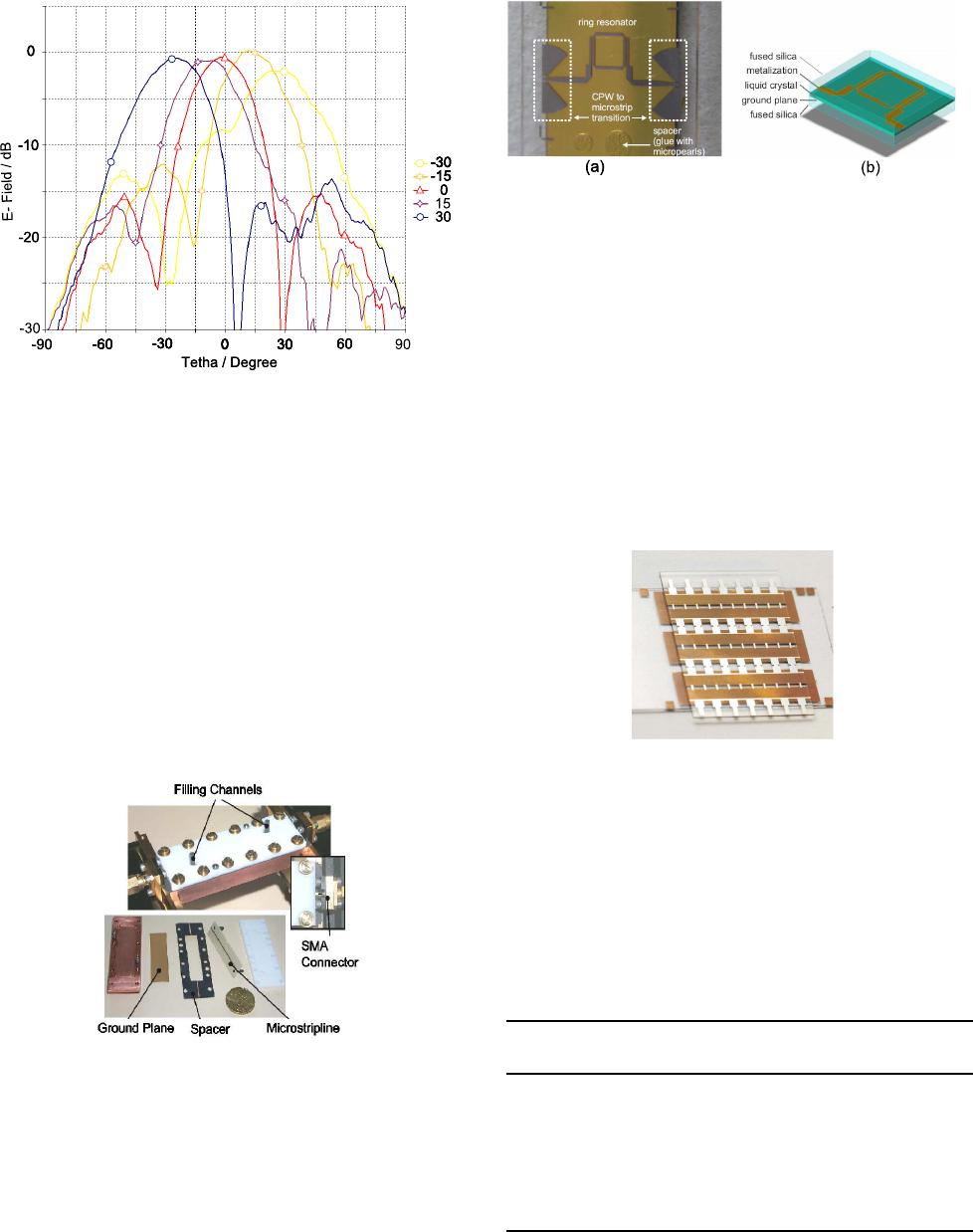
Figure 8. Mesasured E-Plane power pattern of the recon-
figurable patch array
even more by increasing LC cavity height whereas this in-
creases switching time of the phase shifter (Table 1). Fur-
thermore, the IMSL topology has less tuning efficiency
which is defined as a ratio between achievable differential
phase shift (∆φ) over phase shifter length with respect to
λ
0
. For instance, for array antennas, one unit cell size
is about λ
0
/2 x λ
0
/2 . If a meander IMSL type phase
shifter is fabricated in such a limited area, the achievable
differential phase shift is around 280
◦
depending on LC.
This limits the scanning range of the antenna. Thus, due
to low IL, IMSL phase shifter improves G/T whereas lim-
its beam steering speed and wide range of scanning of an
antenna.
Figure 9. Realized IMSL phase shifter
Using a tunable filter [15], i.e. ring resonator as shown
in Fig. 10, the tuning efficiency can be increased. The
reason for this is the compactness of the ring resonator.
Therefore, a phase shifter with diffirential phase shift of
360
◦
can be easily fabricated in a limited area by which
wide range of scanning becomes possible. On the other
hand, being a resonance structure, this topology has high
insertion loss. This leads to a degradation in G/T.
A compromise between low insertion loss, fast beam
steering speed and wide range of scanning can be
Figure 10. Ring Resonator (a) Photograph from the back-
side (b) Three dimensional CAD model
achieved using a loaded line phase shifter [16] as shown
in Fig. 11. This topology is realized using CPW lines
as non-tunable line segments and LC filled parallel plate
capacitors as tunable elements. It has two main improve-
ments compared to previous topologies. First, the inser-
tion loss is reduced. This is caused by the fact that the
RF field is concentrated on the low loss substrate at the
non-tunable segment. Hence, G/T of an antenna can be
increased. Second, switching time is reduced due to the
thin LC layer of the parallel plate capacitors. Therefore,
beam steering speed of an antenna system is increased.
Figure 11. Photograph of Loaded CPW Phase Shifter
Characteristics of these three topologies are given in de-
tail in Table 1. It should be noticed that all three topolo-
gies have a similar fabrication process as given in sec-
tion 2 (Fig. 2). This makes them cost effective when com-
pared to other tunable phase shifter technologies.
Table 1. Comparison of LC Based Planar Phase Shifters
IMSL Resonator Loaded CPW
Parameters [14] [15] [16]
Frequency / GHz 20 34.3 20
Lenght / λ
0
3.3 0.23 0.87
∆φ /
◦
260 117 120
IL / [dB/mm] 0.046 1.91 0.12
FoM / [
◦
/dB] 113 30.6 60
LC layer / µm 254 100 4
LCs have relatively high switching time compared to
other tunable device technologies. This switching time
depends on LC material, its thickness, temperature and
orientation mechanisms. In general, two main mecha-
nisms are used in order to orient LC molecules. These
are mechanically rubbed polyimide film and electrostatic
field. The rubbing generates micro-grooves along the
rubbing direction [5]. When LC is placed on such a
surface, it is aligned parallel to the grooves. This way
of alignment increases switching time. For instance, the
switching time is measured as 92 ms, for a varactor with
a LC layer thickness of 5µm. On the other hand, when
the electrostic field is used, the switching time is 22 ms.
Beside the orientation mechanism, LC layer thickness
has significant impact on the switching time. A varactor
with 1µm LC layer thickness requires 4 ms to align LC
molecules when the polyimide film is used. This value is
reduced to 1 ms if the electrostatic field is used.
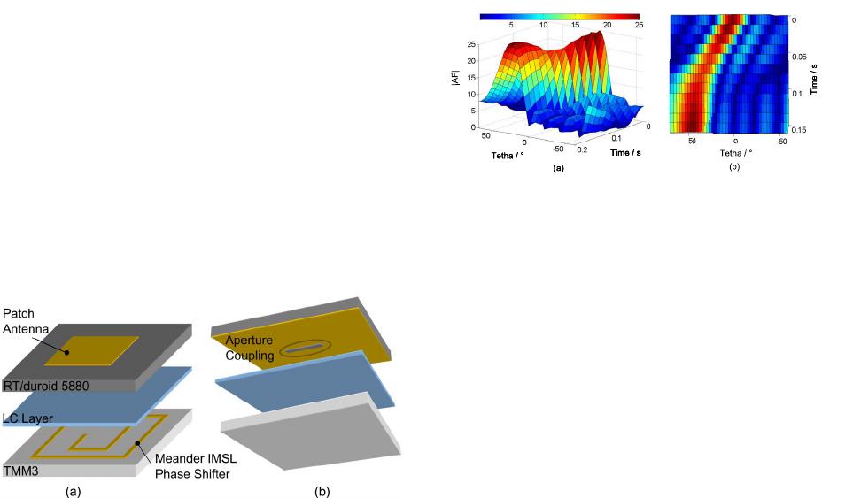
4.2. Microstrip Patch Antenna
In this part CST M icrowave Studio simulation re-
sults of a reconfigurable microstrip patch antenna are pre-
sented for Ka-band. An antenna consists of three dielec-
tric layers is designed. These layers are RT/duroid 5880,
LC and TMM3 as shown in Fig. 12. There are 25 x 25
patch elements and therefore the overall size of the an-
tenna is 20 cm x 20 cm x 1 cm. Meander IMSL phase
shifters with 360
◦
differential phase shift are used and
they are coupled to the radiating elements via aperture
coupling. Bandwidth and radiation efficiency of one unit
cell are determined as 6 % and −0.62 dB, respectively.
The antenna gain is about 25 dB and the main beam di-
rection can be scanned ± 60
◦
in elevation plane in the
absence of mutual coupling.
Figure 12. Expanded views of one unit cell (a) Top-
perspective view (b) Bottom-perspective view
It is a challenge to design an antenna architecture where
LNAs are placed between antenna elements and phase
shifters using LC technology. Therefore, by assuming
that the LNAs are located behind the phase shifters, G/T
can be calculated to 1.6 dB/K for a system with the fol-
lowing values: array gain = 30 dB, antenna noise tem-
perature = 50 K, phase shifter insertion losses = 5 dB,
ambient temperature = 290 K, LNA gain = 20 dB and
LNA noise figure = 4 dB. All expenses of such a system
is mainly determined by the cost of LNAs. The cost of
the antenna and phase shifters can be compared with that
of a LCD which is 20 cm x 20 cm in size.
Effects of the high LC switching time on the antenna per-
formance have to be studied. Optimizations on beam
forming algorithms and phase distribution over the an-
tenna can be performed. However, significant improve-
ment has been achieved by customizing phase shifter
topologies. For instance, the beam steering speed is
around 1
◦
/s empirically if IMSL type phase shifters are
used. This value can be increased up to 200
◦
/s and
higher using a CPW loaded line phase shifter because of
the thin LC layer (Table 1).
Array factor (AF) over time is given in Fig. 13 for a sce-
nario of steering the main beam from 0
◦
to 4 5
◦
in eleva-
tion plane. Although an optimum AF with high directiv-
ity and high side lobe level can be achieved after 0.1 6 s,
the antenna can still get signal from 45
◦
even after 0.1 s.
In this case, the side lobe level is lower than the optimum
value because the phase shifters have not reached their
desired differential phase values.
Figure 13. Array factor (AF) of a 5 x 5 antenna array
over the time (a) Perspective view (b) Top view
5. CONCLUSION AND DISCUSSION
This paper presents the fundamentals of LC material and
its applications for reconfigurable antenna arrays like re-
flectarrays and phased arrays. The most critical issue was
the dielectric loss tangent of this material which was re-
duced with interdisciplinary cooperations with materials
scientists and chemists. Achieved results up to now show
that LC is a promising material for microwave applica-
tions in terms of device performance and cost. Reconfig-
urable reflectarray was presented for Ka-band (and also
fabricated for W-band). These antennas are suitable and
compact solutions for satellite antennas due to their pla-
narity, low mass and low manufacturing cost with respect
to parabolic reflector. For end user antennas, i.e. auto-
motive electronically steerable antennas being integrated
onto a car body, it is preferable to use phased arrays due
to low profile. Tunable planar phase shifters are signif-
icant for multi-layer phased arrays. Thus, these phase
shifters are discussed in details in order to figure out how
they affect antenna performances like G/T, beam steer-
ing speed and wide range of scanning. LC technology is
a cost effective solution for commercial micro- and mm-
wave tunable devices because the required technology for
fabrication of these devices is relatively simple as other
technologies.